- 您现在的位置:买卖IC网 > Sheet目录317 > C8051T610DB24 (Silicon Laboratories Inc)DAUGHTER BOARD T610 24QFN SOCKET
�� �
�
�C8051T610/1/2/3/4/5/6/7�
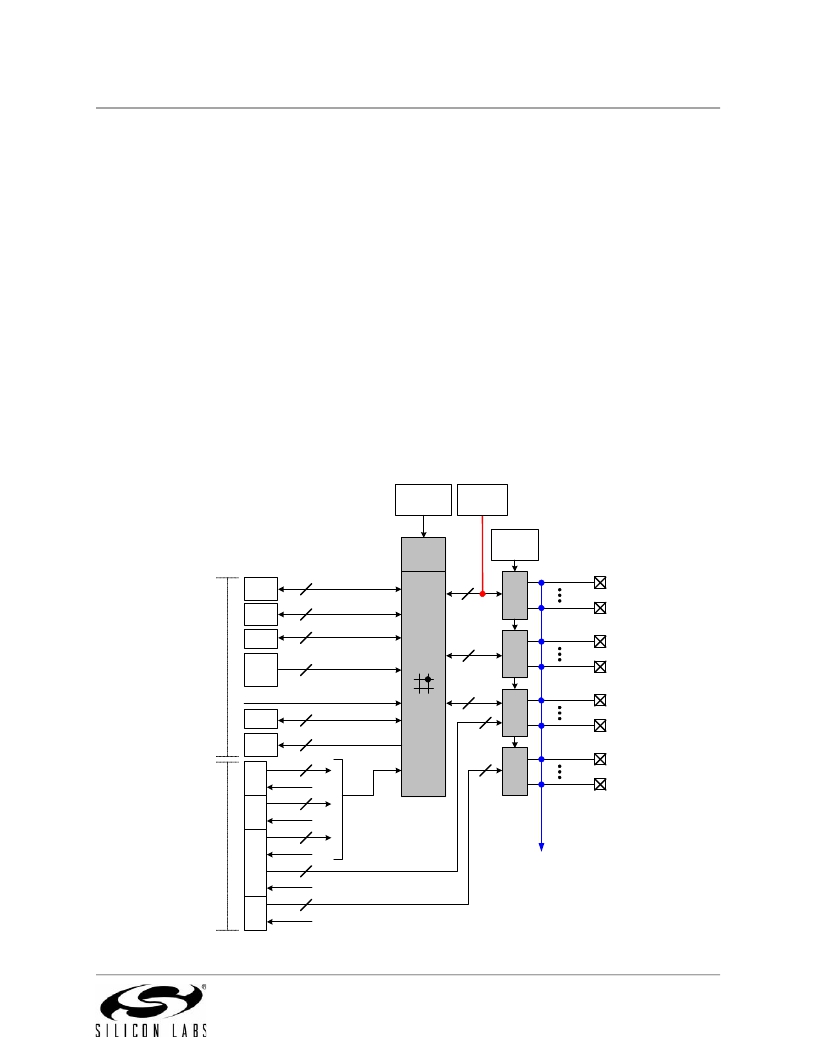
�21.� Port� Input/Output�
�Digital� and� analog� resources� are� available� through� 29� I/O� pins� organized� as� three� byte-wide� ports� and� one�
�5-bit-wide� port� on� the� C8051T610/2/4.� The� C8051T611/3/5� devices� have� 25� I/O� pins� available,� organized�
�as� three� byte-wide� ports� and� one� 1-bit-wide� port.� The� C8051T616/7� have� 21� I/O� pins� available� on� a� single�
�byte-wide� port,� two� 6-bit-wide� ports,� and� a� 1-bit-wide� port.�
�Port� pins� can� be� defined� as� general-purpose� I/O� (GPIO),� assigned� to� one� of� the� internal� digital� resources,�
�or� assigned� to� an� analog� function� as� shown� in� Figure� 21.3.� Port� pin� P3.0� is� shared� with� the� C2� Interface�
�Data� signal� (C2D).� The� designer� has� complete� control� over� which� functions� are� assigned,� limited� only� by�
�the� number� of� physical� I/O� pins.� This� resource� assignment� flexibility� is� achieved� through� the� use� of� a� Prior-�
�ity� Crossbar� Decoder.� Note� that� the� state� of� a� Port� I/O� pin� can� always� be� read� in� the� corresponding� Port�
�latch,� regardless� of� the� Crossbar� settings.�
�The� Crossbar� assigns� the� selected� internal� digital� resources� to� the� I/O� pins� based� on� the� Priority� Decoder�
�(Figure� 21.3,� Figure� 21.4,� and� Figure� 21.5).� The� registers� XBR0� and� XBR1,� defined� in� SFR� Definition� 21.1�
�and� SFR� Definition� 21.2,� are� used� to� select� internal� digital� functions.�
�All� Port� I/O� pins� are� 5� V� tolerant� (refer� to� Figure� 21.2� for� the� Port� cell� circuit).� The� Port� I/O� cells� are� config-�
�ured� as� either� push-pull� or� open-drain� in� the� Port� Output� Mode� registers� (PnMDOUT,� where� n� =� 0,1,2,3).�
��XBR0,� XBR1,�
�PnSKIP�
�Registers�
�Priority�
�Decoder�
�External�
�Interrupts�
�EX0� and� EX1�
�PnMDOUT,�
�PnMDIN�
�Registers�
�Highest�
�Priority�
�UART�
�SPI�
�2�
�4�
�8�
�P0�
�I/O�
�Cells�
�P0.0�
�P0.7�
�2�
�SMBus�
�CP0,�
�CP1�
�4�
�Digital�
�Crossbar�
�8�
�P1�
�I/O�
�Cells�
�P1.0�
�P1.7�
�Outputs�
�SYSCLK�
�4�
�P2�
�P2.0�
�Lowest�
�Priority�
�PCA�
�T0,� T1�
�6�
�2�
�8�
�4�
�5�
�I/O�
�Cells�
�P3�
�P2.7�
�P3.0�
�I/O�
�P0�
�(P0.0-P0.7)�
�Cells�
�P3.4�
�8�
�P1�
�(P1.0-P1.7)�
�4�
�(P2.0-P2.3)�
�P2�
�P3�
�4�
�(P2.4-P2.7)�
�5�
�(P3.0-P3.4)�
�To� Analog�
�Peripherals�
�Figure� 21.1.� Port� I/O� Functional� Block� Diagram�
�Rev� 1.1�
�113�
�发布紧急采购,3分钟左右您将得到回复。
相关PDF资料
C8051T630DB20
BOARD SOCKET DAUGHTER 20-QFN
CAN-100
BOARD EVAL RS232 100QFP
CANADAPT28
KIT ADAPTER CANDEMOBOARD 28PLCC
CAT24AA01WI-GT3
IC EEPROM SERIAL 1KB I2C 8SOIC
CAT24AA02WI-G
IC EEPROM SERIAL 2KB I2C 8SOIC
CAT24C01ZI-G
IC EEPROM SERIAL 1KB I2C 8MSOP
CAT24C03WI-G
IC EEPROM SERIAL 2KB I2C 8SOIC
CAT24C04ZI-G
IC EEPROM SERIAL 4KB I2C 8MSOP
相关代理商/技术参数
C8051T610DB28
功能描述:子卡和OEM板 C8051T610 Family Socket Daughtr Board RoHS:否 制造商:BeagleBoard by CircuitCo 产品:BeagleBone LCD4 Boards 用于:BeagleBone - BB-Bone - Open Source Development Kit
C8051T610DB32
功能描述:子卡和OEM板 C8051T610 Family Socket Daughtr Board RoHS:否 制造商:BeagleBoard by CircuitCo 产品:BeagleBone LCD4 Boards 用于:BeagleBone - BB-Bone - Open Source Development Kit
C8051T610DK
功能描述:开发板和工具包 - 8051 C8051T610 Series Development Kit RoHS:否 制造商:Silicon Labs 产品:Development Kits 工具用于评估:C8051F960, Si7005 核心: 接口类型:USB 工作电源电压:
C8051T610-GQ
功能描述:8位微控制器 -MCU 16KB 10ADC 32Pin MCU RoHS:否 制造商:Silicon Labs 核心:8051 处理器系列:C8051F39x 数据总线宽度:8 bit 最大时钟频率:50 MHz 程序存储器大小:16 KB 数据 RAM 大小:1 KB 片上 ADC:Yes 工作电源电压:1.8 V to 3.6 V 工作温度范围:- 40 C to + 105 C 封装 / 箱体:QFN-20 安装风格:SMD/SMT
C8051T610-GQR
功能描述:8位微控制器 -MCU 16KB 10ADC 32Pin MCU RoHS:否 制造商:Silicon Labs 核心:8051 处理器系列:C8051F39x 数据总线宽度:8 bit 最大时钟频率:50 MHz 程序存储器大小:16 KB 数据 RAM 大小:1 KB 片上 ADC:Yes 工作电源电压:1.8 V to 3.6 V 工作温度范围:- 40 C to + 105 C 封装 / 箱体:QFN-20 安装风格:SMD/SMT
C8051T611-GM
功能描述:8位微控制器 -MCU 16KB 10ADC 28Pin MCU RoHS:否 制造商:Silicon Labs 核心:8051 处理器系列:C8051F39x 数据总线宽度:8 bit 最大时钟频率:50 MHz 程序存储器大小:16 KB 数据 RAM 大小:1 KB 片上 ADC:Yes 工作电源电压:1.8 V to 3.6 V 工作温度范围:- 40 C to + 105 C 封装 / 箱体:QFN-20 安装风格:SMD/SMT
C8051T611-GMR
功能描述:8位微控制器 -MCU 16KB 10ADC 28Pin MCU RoHS:否 制造商:Silicon Labs 核心:8051 处理器系列:C8051F39x 数据总线宽度:8 bit 最大时钟频率:50 MHz 程序存储器大小:16 KB 数据 RAM 大小:1 KB 片上 ADC:Yes 工作电源电压:1.8 V to 3.6 V 工作温度范围:- 40 C to + 105 C 封装 / 箱体:QFN-20 安装风格:SMD/SMT
C8051T612-GQ
功能描述:8位微控制器 -MCU 8KB 10ADC 32Pin MCU RoHS:否 制造商:Silicon Labs 核心:8051 处理器系列:C8051F39x 数据总线宽度:8 bit 最大时钟频率:50 MHz 程序存储器大小:16 KB 数据 RAM 大小:1 KB 片上 ADC:Yes 工作电源电压:1.8 V to 3.6 V 工作温度范围:- 40 C to + 105 C 封装 / 箱体:QFN-20 安装风格:SMD/SMT